


Additive manufacture (AM), and in particular the powder bed fusion (PBF) process, has offered hope to manufacturing industries needing to meet the environmental and economic targets of global industry sectors and the corresponding guidelines and regulations. Indeed, AM offers a disruptive capability in this regard, but user uptake has been slower than envisaged as difficulties with its implementation have surfaced time and again, and more traditional production technologies have won the argument.
AM is no different to any other manufacturing process that relies on the interaction between a manufacturing system and the material of the product being manufactured. For that interaction between the system and the material to be simultaneously understood, repeatable, and to deliver the required output, clear and consistent knowledge of both the system and the raw material is essential. The process owner has to bring these two halves together to ensure the whole.
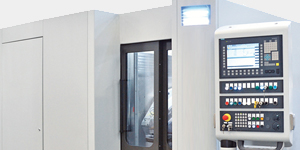
Wayland Additive understands this need from the user’s perspective and has made it its mission to develop a machine that allows the user full, repeatable, and safe control of a metal AM process.
To do this, two things are essential in the machine architecture:
- It must present to the user a stable platform (machine and process material).
- It must also be capable of great flexibility and control to accommodate the wide range of user applications.
However, stability and flexibility have not always comfortably complemented each other in the field of AM. Wayland Additive is operating to break this barrier down.

Focusing on eBeam
The physics of the electron beam (eBeam) process is ideally suited for AM. Electron beams have been used for decades in precision welding, in scanning electron microscopy, and in the semiconductor industry for mask manufacture and direct writing of nanopatterns onto resists — with each application putting its own unique demands on the technology.
Feature size and process capability is a function of the alliance between the raw material (or in the case of electron microscopy, the sample) and the machine. AM is no different.
Lacking Stability
When the Wayland team first closely reviewed additive processes (back in 2015) it was struck by the lack of stability exhibited both in the machines and the output. The team’s attention turned to the PBF (powder bed fusion) process, where laser and eBeam machines were operating and where repeatability from part-to-part and from build-to-build was lacking at the system level and from part-to-part at the output level. This was a consequence of both process issues and the constraints of existing machine capabilities. Each of the two competing energy sources brought their own unique challenges for users looking to achieve successful outcomes.
With the laser PBF process, residual thermal stress, soot contamination, low productivity, the challenge of process monitoring, limited part volume, and limited process control parameters restrict the process dynamics and the optimization options available to the user. This, in turn, has led to machine makers and customers turning to material scientists to develop new materials dedicated to the AM process in an attempt to overcome such limitations. It is interesting to note that huge sums of money are now being spent in the industry trying to develop “forgiving” materials in order to get around the issues presented by both laser PBF and traditional eBeam PBF systems. This may be one way of solving the problem, but the strategy of relying on bespoke materials for targeted applications may further add to the cost of AM. Powder producers need to be able to produce large volumes in order to reduce costs, rather than providing a wide range of specialist alloys.
With the eBeam process, the problem of powder charging — that alliance between the machine and the material — meant that the process stability and breadth were immediately and severely compromised.
With a background in electron beam systems, the Wayland team reviewed the state-of-the-art and immediately set about removing the constraints from the eBeam process, believing that the physics of the process is fundamentally more favorable to AM in the following ways:
- The energy transfer from the electron beam to the powder is a kinetic process.
- Extremely fast deflection speeds can be achieved as there are no mirrors to manipulate.
- The incident power on the powder bed is easily measured and controlled.
- There are no optical surfaces between the electron source and the powder bed to contaminate and deteriorate with time.
- The process can run hot and so take place above the annealing temperature of the process material, resulting in stress free parts with less post processing.
- The process takes place in a vacuum so powder contamination and oxidation is reduced and powder life extended.
- In-process monitoring can take place using a range of photon and electron detectors and systems.
Electrons have an inherent advantage over photons in that they are charged particles, which means the beam can be deflected, focused, and corrected very rapidly without any physical contact, scattering, or absorption. Within the context of AM to date, however, this has also proved to be a disadvantage. When charged particles are incident upon insulating materials, they tend to adhere and build up a surface charge. When this happens during the metal eBeam AM process (where the accelerating potential of the electrons is many thousands of volts and metal powders tend to have an insulating surface oxide layer), a considerable potential can build up on the powder bed until the powder particles are caused by Coulomb forces to repel each other and a “smoke event” occurs. When this happens, the particles become free flying within the chamber, and the build is violently terminated, potentially to the detriment of the machine as well as the build. This build-up of charge occurs very rapidly and has to be managed throughout the build process in order to reliably complete a build.
To date, the accepted way of overcoming this problem is to lightly sinter the powder together from the start of the build, layer-by-layer, across the entire build platform, with the consequence that the end product being manufactured is encased in a block of sintered powder that needs to be blasted off. Finding the right conditions to create and maintain a reliable sinter process can be challenging, and the advantages outlined earlier in relation to the physics of the electron beam process are all spent in achieving a process that allows reliable sintering of the powder bed rather than being used to optimize the build parameters for the part being produced. The many control levers in an electron beam system are therefore largely out of bounds as only a narrow and limited range of parameters allow the user to create both a sinter cake and a fully dense part.

NeuBeam Ensures Stability is Built-in
The electron beam and charged particle physics and engineering expertise gathered at Wayland has allowed it to look not only at the aspects that dictate basic machine stability such as high-voltage performance, vacuum integrity and cleanliness, electromagnetic shielding, beam-deflection capability, distortion corrections, and noise, but also at the limiting process issues (i.e. powder charging) in order to develop a system that offers the user a stable yet broad process window for product development across a breadth of materials. The user will no longer walk the tightrope of compromise, but rather hasten along a stable path of product development. The latter achieved by overcoming the charge accumulation of electrons on the powder bed, without the need to pre-sinter the powder, thereby creating a stable process that allows the capability of the electron beam to explore/exploit the material properties of the metal and to manipulate the thermal rates of change within the melt pools.
The NeuBeam process and the new Wayland system have been designed from the bottom up and incorporate many years of learning from the semiconductor industry — a hard task master. The team listened to the experiences of users of metal AM platforms and, in so doing, realized they did not need to invent a new wheel but rather adapt an existing and sophisticated capability built on hard-won knowledge from another field (the semiconductor industry). By combining these experts with long-term AM industry insiders, it was possible to rapidly develop both the machine and the processes, and so the marriage of machine and process was established from the beginning.

Without the need to pre-sinter and without the problem of powder charging, the NeuBeam process presents a new capability to the AM arsenal:
It is stable: It will allow the full range of AM powder sizes to be used while processing above the annealing temperature of the material.
It is clean: The “soot” problem present in laser systems requiring the cross flow of an inert gas to prevent powder bed contamination does not exist. The process takes place under vacuum, so there is less contamination of powder and, therefore, greater powder recyclability. The power delivery from the electron emitter to the powder bed is through free space, and there is no contact with influencing surfaces.
It is fast: Electromagnetic deflection systems can move the beam in the thousands-of-meters-per-second regime. This fast-deflection capability means higher-beam powers can be used, which speeds up build times and ensures good control over the thermal properties of the build.
It is simple: Build supports are minimal, thermal stresses are not a consideration, powder can freely flow out of the build with only minor de-powdering needed, wire erosion is not needed to cut the build off the start plate, and post-build heat treatments are not required.
It is efficient: The component being built is thermally isolated from its surrounding, so less power is needed to keep the part temperature above the annealing temperature.
It is adaptive: New materials can be rapidly developed, and in-process monitoring enables near real time process control.
In short, NeuBeam offers a manufacturing process that is both stable, flexible, and adaptable.

Stability, often achieved at the expense of flexibility, goes hand-in-hand with flexibility in the Wayland machine. Often users of metal AM systems find themselves constrained to a process with little-to-no flexibility. Melt parameters are locked down, material processing themes are restricted, and the machines are presented as a black box, not open to scrutiny and/or experimentation. With the NeuBeam process, Wayland intends to demonstrate this does not have to be the case.
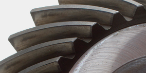
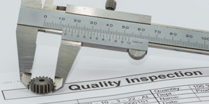
Due to the nature of the NeuBeam process, the route from CAD to finished, post-processed part is simplified. NeuBeam results in easy powder removal, no requirement for post-build heat treatment to remove residual stress, and no requirement to wire erode the part off the start plate. Subtractive post processing of the part is also simplified. Studies by the Wayland team using NeuBeam technology to make precision AQ10 to AQ14 aerospace gears using AM produced blanks proved that high-precision components were achievable with the added AM advantage of shape complexity. The AM blanks were stable throughout the subtractive machining steps and maintained their form in use. Precision gears were manufactured with no additional special tooling or fixturing. With the NeuBeam process, the ability to produce the blank in any orientation meant the metallurgy and microstructure could be aligned to the load paths of the gear teeth, potentially enhancing performance for lightweight systems.
The stability of the Wayland machine in terms of process and performance means the breadth of the eBeam control parameters are accessible to the user. In addition, the boundaries of stable operation are much further out, and so much more process optimization can be achieved. This increases the scope for the user in terms of how they run the machine. When the first machine is launched early next year, Wayland intends to provide material parameter sets for quick start builds; however, users will also be encouraged to get familiar with the machine control parameters, to experiment, and to learn and develop, thereby strengthening the marriage between machine and process, which is so important for rapid-product development, pilot production, and higher-volume production. During this process, Wayland will support its customers on their journey with application, process, and machine expertise.
The Wayland machine, designed for production but with the front-end process development activity in mind, should enable the seamless transfer of parts from development to production, from R&D to manufacturing. The Wayland machine will not present as a black box but will allow the process engineers to ply their trade and the production managers to lock down processes, qualify output, and control their schedules.


